TouchDRO Adapter Comparison
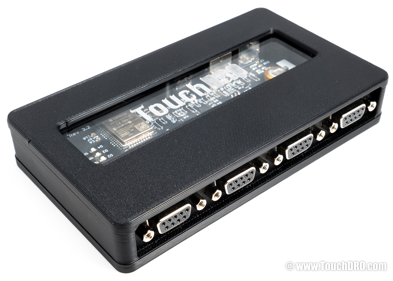
TouchDRO adapter boards connect your DRO scales to the TouchDRO Plus Android app over Bluetooth, turning a tablet into a full-featured digital readout for your milling machine or metal lathe. There are two product families:
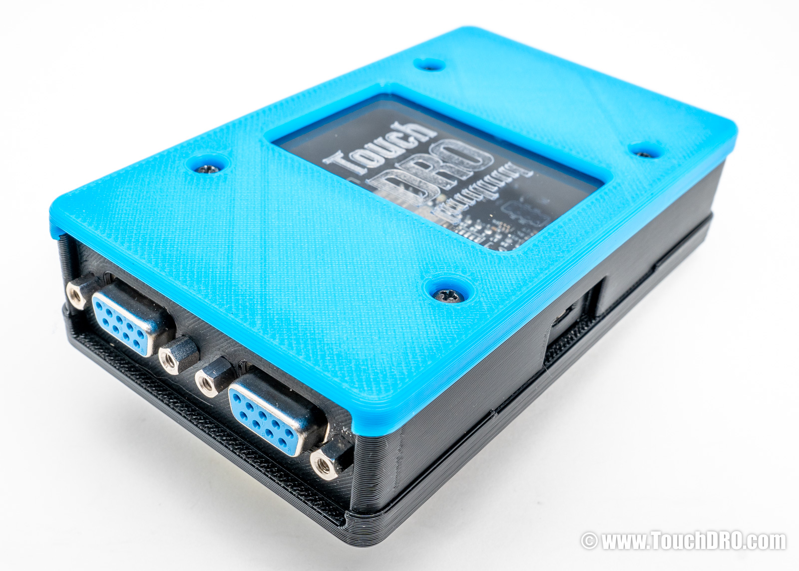
- Pre-assembled adapters — the TDA-420 (milling machines) and TDA-410 (metal lathes) come ready to use with a 5-year warranty, touch probe and reference mark support, and power-loss position backup.
- DIY kit — the TDK-40 is budget-friendly and easy to build, with the same core architecture and tachometer input.
Both families run the same core firmware and share the same input architecture. All models include four high-speed differential scale inputs and work with the majority of modern glass, magnetic, and inductive DRO scales. iGaging and Mitutoyo SPC scales are supported via signal converter modules (sold separately).
Adapter Features
| TDA-420 | TDA-410 | TDK-40 | |
|---|---|---|---|
 |
 |
||
| Comes fully assembled. Learn more | Requires some soldering and mechanical assembly. Learn more | ||
| Best For | Milling Machine | Metal Lathe | Milling Machine or Lathe |
| Price | From $299 | From $259 | From $99 |
| Inputs | |||
| Total Inputs | 6 | 4 | 4 |
| RS-422/Differential Inputs | 4 | 4 | |
| TTL/Single Ended Inputs | 2 1 | 1 | 0 |
| Reference Track Support | Yes 2 | No | |
| Serial Protocol Decoding | iGaging, Mitutoyo SPC, BIN6 3 | ||
| Tachometer Input | Yes 1 | Yes | Yes |
| Probe/Height Setter Inputs | 2 1 | No | No |
| Limit Switch Inputs | 4 1 | 2 1 | No |
| Connectivity | |||
| Bluetooth | Yes | ||
| USB | Standalone + Bluetooth mirror | Bluetooth mirror only | |
| Other Features | |||
| TouchDRO Version | TouchDRO Plus | ||
| Power Loss Position Retention | Yes | No | |
| Over-the-Air Updates | Yes | ||
| Warranty | 5 years | No Warranty | |
| Returns | 30 days, like-new condition | 30 days, unsoldered | |
1 The flexible TTL inputs can be user-configured as a combination of up to one/two encoder inputs (TDA-410/420), pair of probe inputs (TDA-420), tachometer input, or one or two pairs of limit switch inputs (TDA-410/420).
2 Requires DRO scales with a compatible reference track.
3 Requires a compatible signal converter module.
Technical Characteristics
| TDA-420/410 | TDK-40 | |
|---|---|---|
| Position Refresh Rate | 25Hz | |
| Supply Voltage | 5V-5.5V | |
| Max Current Draw | 300mA | |
| Firmware Family | ESP32 V3 | |
| Primary Scale Inputs | ||
| Input Lines per Axis | A, A', B, B', R/Z, R'/Z' | A, A', B, B' |
| Encoder Support | PNP, NPN, Push/Pull | |
| Supply Voltage | 5V | |
| Min Signal Voltage | 1.8V | |
| Max Signal Voltage | 5V | |
| Max "Low" Signal Voltage | 1.2V | |
| Min "High" Signal Voltage | 3.6V | |
| Max Input Frequency | 1MHz | |
| Min Edge Separation | 250ns | |
| Glitch Rejection | Yes | |
| Reference Trigger Latency | 2 µs | N/A |
| Aux. Axis Inputs | ||
| Input Lines per Axis | 2a | 0b |
| Encoder Support | NPN, Push/Pull | N/A |
| Supply Voltage | 5V | |
| Min Signal Voltage | 2V | |
| Max Signal Voltage | 5V | |
| Max Low Signal Voltage | 1V | |
| Pull up/down | Pulled up to 5V | |
| Max Quadrature Frequency | 100KHz | N/A |
| Min Quadrature Edge Separation | 5 µs | N/A |
| Glitch Rejection | No | N/A |
| Tachometer Pulses/Second | 0.5-40,000 | |
| Max Probe Latency | 2 µs | N/A |
| Max Limit Switch Latency | 2 µs | N/A |
aTDA-420 only
bTDA-410 does not support auxiliary axis inputs
Understanding the Specs
Position Refresh Rate
The frequency at which the adapter sends position updates to the app while an axis is in motion. All current-generation adapters update at 25 times per second.
Max Frequency
Highest quadrature signal frequency that the input will be able to process; higher is better. Exceeding this frequency will lead to missed pulses. For example, a 1-micron scale moving at 1 meter per second will have quadrature frequency of 250KHz.
Min Edge Separation
Minimum pulse width that the adapter will register; lower is better.
Tachometer Pulses Per Second
This is the number of pulses per second the tachometer can recognize reliably. For instance, when a single mark encoder disk is used, the tachometer will read between 30 RPM and 600,000 RPM (1 pulse every 2 seconds to 10,000 pulses per second); with a disk that has 10 marks, the supported RPM range will be between 3RPM and 60,000 RPM.
Probe and Limit Switch Trigger Delay
This is the amount of time the adapter will take to capture the position after the probe or a limit switch is engaged. Lower is better. This is proportional to the potential digital "backlash" in the system. For instance, when the axis is moving at 1mm per second, 1µs delay will result in potential error of 0.000001mm; 100ms will result in 0.1mm potential error.
Max Signal Voltage
This is the highest safe signal level that can be applied to the given input. Voltage that is higher than the indicated level will quickly permanently damage the input and the board will need to be repaired.
Min Signal Voltage
This is the lowest voltage level that will be recognized by the given input. Any value above this level (up to the max voltage) will be treated as a logical 1.
Max Low Signal Voltage
This is the highest voltage level that will still be recognized as a logical 0 when the signal is going from high-to-low.
Frequently Asked Questions
[Expand]Can I use the lathe adapter (TDA-410) on a mill, or the mill adapter (TDA-420) on a lathe?
Yes. The TDA-410 and TDA-420 are functionally identical—same board, same firmware. The only difference is that the TDA-420 has one additional flexible TTL input, which provides the touch probe and extra limit switch connections useful on a milling machine. Either adapter will work on either machine. If you're unsure, the TDA-420 gives you the most flexibility.
I have a mill and a lathe—do I need two adapters?
Yes, each machine needs its own adapter. But they share the same app—you can switch between machines on one tablet by selecting the appropriate Bluetooth connection.
Can I start with the DIY kit and upgrade to a pre-assembled adapter later?
Yes. The kit and the TDA adapters use the same app and work with the same scales. Your scales, tablet, and TouchDRO Plus license all carry over. If you later want touch probe support, power-loss position backup, or a warranty, you can add a TDA adapter without replacing anything else in your setup.
Do I really need the touch probe input?
It depends on your workflow. If you regularly edge-find or zero off a reference surface, a touch probe saves significant time and improves repeatability. If you mostly work from existing datums or use manual edge finders, you won't miss it. The probe input is only available on the TDA-420.